TFT Flat-Panel Array Image Acquisition
Objectives
On completion of this chapter, you should be able to:
• Define a thin-film transistor (TFT) flat-panel digital image detector.
• Describe the construction of direct and indirect TFT flat-panel detector systems.
• Differentiate between direct and indirect image capture.
• Describe a gadolinium oxysulphide (Gd2O2S) detector.
• Describe a thallium doped cesium iodide (CsI[TI]) detector.
• Relate the design of a TFT flat-panel detector to its performance measurements.
• Describe the cause of image lag and the process of correcting.
Key Terms
Active-matrix flat-panel imagers (AMFPI)
Direct conversion
Field effect transistor (FET)
Flat-panel detector
Gadolinium oxysulphide (Gd2O2S)
Gain calibration
Hydrogenated amorphous silicon (a-Si:H)
Image artifacts
Image lag
Indirect conversion
Offset correction
Photoconductors
Sensing component
Switching component
Thallium doped cesium iodide (CsI[TI])
Thin-film transistor (TFT)
The first thin-film transistor (TFT) flat-panel amorphous silicon and amorphous selenium detectors were introduced in 1995. These were the first devices to move beyond the cassette into detectors that would reside in the table and wall stand. Today these detectors are no longer permanent fixtures in these two pieces of equipment but can be used portably as a wireless device. With flat-panel detectors, the materials used for detecting the x-ray signal and the sensors for recognizing that signal are permanently enclosed inside a rigid protective housing. This chapter will explore these devices and differentiate between the two major types of x-ray signal conversion: indirect and direct.
Active-Matrix Flat-Panel Imagers
Active-matrix flat-panel imagers (AMFPI) consist of a flat-panel array with an x-ray absorption material. The two main types of x-ray absorption materials currently being used are photoconductors and scintillators. Photoconductors are materials that absorb x-rays, resulting in an electrical charge. Scintillators are phosphors that produce light when absorbing x-rays. An AMFPI detector measures the response of these materials to x-ray absorption and is a large area two-dimensional (2-D) array of pixels fastened to a thin glass backing, or substrate. The absorption material is attached to the surface of this array either electrically, as in the case of the photoconductor, or physically, as in the case of the phosphor material. The 2-D array functions as a very efficient device that measures x-ray absorption rather than counting or measuring the actual x-rays. The choice of x-ray absorption material determines whether the detector is direct conversion or indirect conversion.
Direct Conversion
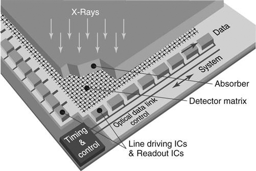
In direct conversion, x-ray photons are absorbed by the coating material and immediately converted into an electrical signal. The flat-panel detector has a radiation-conversion material or photoconductor, typically made of amorphous selenium (a-Se) that is about 500 µm thick for radiography and 200 to 250 µm thick for mammography. This material absorbs x-rays and converts them to electrons, which are stored in the TFT detectors (Figure 5-1). The TFT is a photosensitive array made up of small (about 100 to 200 µm) pixels, also called a detector element (del) in these TFT arrays. Each pixel contains a photodiode that absorbs the electrons and generates electrical charges. A field effect transistor (FET) or silicon TFT isolates each pixel element and reacts like a switch to send the electrical charges to the image processor (Figure 5-2). More than 1 million pixels can be read and converted to a composite digital image in less than 1 second. A line of TFT switches, each associated with a storage capacitor, allows the electrical charge information to discharge when the switches are closed. The information is discharged onto the data columns and read out with dedicated electronics. Specialized silicon integrated circuits are connected along the edges of the detector matrix. On one side, integrated circuits control the line scanning sequence, and on the other side, low-noise, high-sensitivity amplifiers perform the readout, amplification, and analog-to-digital conversion. High-speed digital electronics are then used to achieve fast image acquisition and processing.
Indirect Conversion
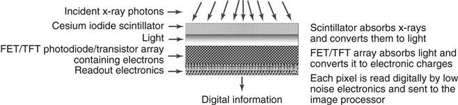
Indirect-conversion detectors are similar to direct detectors in that they use TFT technology. Unlike direct conversion, indirect conversion is a two-step process: x-ray photons are converted to light, and then the light photons are converted to an electrical signal. A phosphor such as gadolinium oxysulphide (Gd2O2S), or thallium doped cesium iodide (CsI[TI]) rapidly absorbs x-rays and produces light. The phosphor layer is known as the scintillation layer. The scintillation layer can be either structured or unstructured. Unstructured layers produce more scattered light than structured layers, thereby decreasing the efficiency of the detector. The light is then converted into an electric charge by a photodetector such as a hydrogenated amorphous silicon (a-Si:H) photodiode array. The two-step process occurs as follows:
Step 2: A photosensitive array, made up of small (about 100 to 200 µm) pixels, converts the light into electrical charges. Each pixel contains a photodiode that absorbs the light from the scintillator and generates electrical charges. A FET or silicon TFT isolates each pixel element and reacts like a switch to send the electrical charges to the image processor. As with direct conversion, more than 1 million pixels can be read and converted to a composite digital image in less than 1 second (Figure 5-3).
Gd2O2S Detectors.
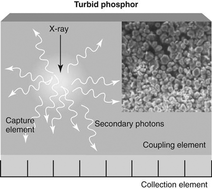
The gadolinium oxysulphide (Gd2O2S) detecting material is made from small crystals bound together in an unstructured or turbid (powdered granules) layer along with a polyurethane material. The crystalline layer is filled with air pockets that allow light that was generated in the phosphor to escape. It also allows light to escape laterally before it reaches the surface, reducing the efficiency of the phosphor and lowering spatial resolution (Figure 5-4). Gd2O2S was used primarily for applications that required a rugged detector, such as portable detectors either wired or wireless. The ruggedness was a result of the unstructured or phosphor layer.
CsI Detectors.
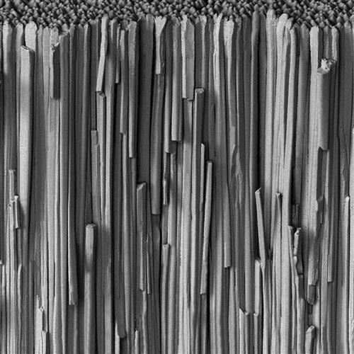
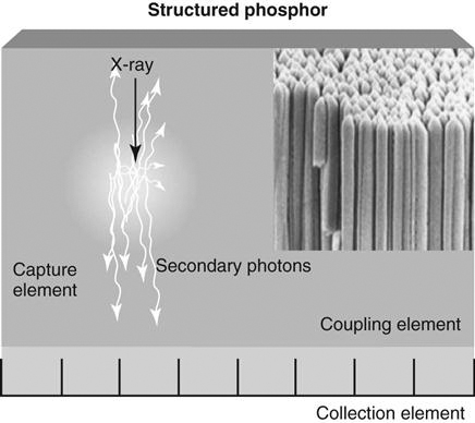
The most popular type of amorphous silicon detector uses a CsI scintillator. The scintillator is made by growing very thin crystalline needles (5 to 10 µm wide) perpendicular to the detector surface; these crystalline needles work as light-directing tubes, much like fiber optics (Figure 5-5). Because of how the cesium iodide crystals are grown, they are considered a structured scintillator. These needles can be evaporated onto the surface of the layer, or they can be grown with a seed layer. This allows greater detection of x-rays (higher detective quantum efficiency DQE than a Gd2O2S scintillator), and because there is almost no light spread, the spatial resolution is higher (Figure 5-6). These needles absorb the x-ray photons and convert their energy into light, channeling it to the amorphous silicon photodiode array. In the past, CsI detectors could not be practically used in a portable-type detector. The crystalline structure was too delicate to be used outside of a protected environment of a fixed detector array. However, today, because of the advances in materials and crystalline formation on the array, both CsI and Gd2O2S are being used in portable detectors.
Flat-Panel Array Design and Performance
Design
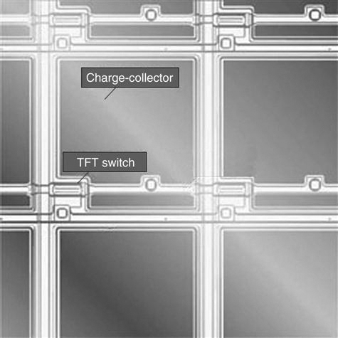
The way an a-Si:H array functions is very complex; however, the design is fairly simple. Each pixel contains a sensing component and a switching component. There are two types of switching components: a 2-contact switching diode and a 3-contact TFT. The sensing component depends on the type of absorbing material and the vendor’s choice of construction. A phosphor/scintillator requires a photodiode or phototransistor to detect the light. If a photoconductor (a-Se) is selected, the sensing element is a capacitor that measures charge. This is also known as a storage capacitor.
To operate, the flat-panel detectors use about 2.5 kilometers or 1.6 miles of electrical bias (a predetermined amount of voltage or current in an electrical circuit), control, and signal output lines laid out on the array surfaces so that each pixel is monitored and refreshed during the control and reading process. Each row of pixels is connected to the same horizontal control line, and each column is connected to the same vertical data line. The readout electronics are attached to the edges of the array, and the entire array and its components are enclosed in a protective housing.
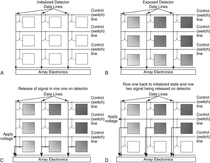
When the exposure is made, the sensing/storage component within the pixel contains the image information. The information is then read out line by line via the changing of the control line voltage so each pixel is connected to its corresponding data line at the bottom of the column (Figure 5-7). Figure 5-7A illustrates the detector in its initialized state, prepared and waiting for exposure. In Figure 5-7B, the detector has been exposed and is awaiting reading of the array. Figure 5-7C demonstrates the readout or release of signal of row one. Notice that a voltage is applied across the control or switch line corresponding to row one. In the final image of Figure 5-7, row one has returned to an initialized state (the process of returning to this state varies per vendor and is beyond the scope of this textbook) after release of its signal and the readout process continues to row two. Once the signal has been released, the energy is then transferred to the electronics that are attached to the edges of the array.
Performance
There are two ways to measure detector performance: (1) numerical measurement of spatial resolution and DQE, and (2) observation of low-contrast objects in a contrast detail phantom. The actual procedures to measure detector performance are beyond the scope of this book; however, current performance measurement of signal-to-noise ratio and DQE support that flat-panel a-Si:H detectors perform better than other digital imaging systems.
Flat-Panel Artifacts
Dead Pixels
There is a possibility in any imaging system of losing or misrepresenting image information because of defects in the operation components of the device. Although not very common, image artifacts can be caused by malfunctions in the detector. Because manufacture of the pixels is so complex, it is inevitable that the array structure will suffer some damage. Dust, scratches, static discharge, chemical corrosion, or interactions between materials can occur, resulting in some defective pixels. These pixels may be malfunctioning or dead, that is, not functioning at all. As the detector ages, the number of dead pixels increases but may not be detected if they are located on the edges of the panel. Manufacturers make efforts to maintain a standard of less than approximately 0.1% to 0.2% defective pixels and build software programs into their systems to identify and isolate dead pixels. The software uses an interpolation method to “fill in” the dead pixels with information using the surrounding pixels as a guide.
Incorrect Gain Calibration
Gain calibration is used to correct flaws in the detector. If an area of the detector has a large amount of dead pixels or if there is an area of the detector that has poor connections between the conversion layer and the a-Si/TFT array, a noticeable artifact can be seen on the screen. To remove the potential of having that artifact interfere with diagnosis, a process known as gain calibration or flat fielding is used. This process will remove these densities on the image by creating a mask of those defects. When a subsequent image is taken, the software will use the mask to remove the unwanted densities and leave only the diagnostic information. Gain calibration should be performed under the same or similar circumstances in which clinical images will be taken. The calibration should be done according to the equipment manufacturer’s guidelines. In Figure 5-8, the automatic exposure control AEC cells appear as slightly positive squares in the image. The gain calibration was performed with the detector outside of the Bucky and then a subsequent image was taken with the detector in the Bucky. This could happen if anything is left on the detector during a gain calibration. These faint marks could lead to a misdiagnosis.
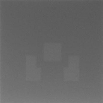
Image Lag and Incorrect Offset Correction
Some flat-panel systems have the ability to take images faster than the detector can accommodate. If an image is taken prior to the detector releasing all of the signal from the previous image, a faint image of the previous exposure may be visible. This is known as image lag. Image lag is almost a double exposure of sorts. When the detector is unable to get rid of all of the signal from the previous image, lag can occur. Rapid succession of images is only one reason for image lag. Another reason image lag might occur is overexposure or an area with little beam attenuation, such as a technologist’s lead marker location. In Figure 5-9, a faint R is visible in the proximal thoracic spinous processes. The R is left over from the previous image. The following techniques can be used to reduce the possibility of image lag:
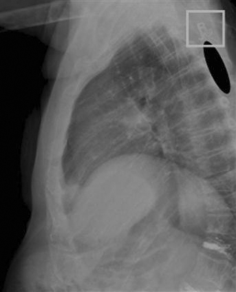
Notice the faint R in the proximal thoracic spinous processes. (Reprinted with permission from the American Journal of Roentgenology.)
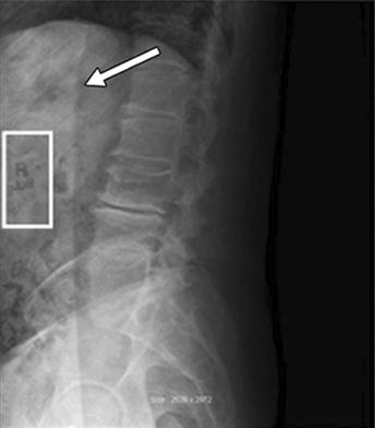
Image lag can also be corrected with the detector’s software using the dark noise or offset correction. Offset correction determines the amount of signal inherent in the detector. If an offset correction is performed prior to residual signal leaving the pixels, that information will be stored as inherent and could cause a negative image of the residual signal. Always follow the equipment manufacturer’s guidelines when performing any detector calibrations. For example, in Figure 5-10 an offset correction was performed after an examination was done with a right side marker in an area of unattenuated radiation. Residual signal remained in that area and a subsequent offset correction was performed. The R is now viewed inversely because that signal created a mask during the offset correction. In Figure 5-10 it is clear that the signal is still very strong and this image was taken 10 minutes after the initial exposure.
Emerging Technology
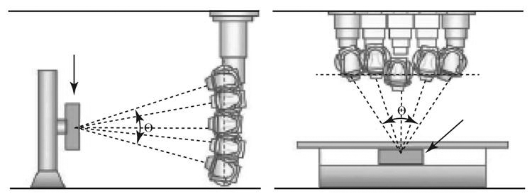
In conventional projection imaging in the past an imaging technique called tomography was used. Tomograms were acquired by attaching a fulcrum to the Bucky and tubehead. The Bucky and tubehead would move in concert with one another and the tube would arc across the patient. The fulcrum point would determine the area in the body imaged. This same concept is now being used in digital imaging and it is called tomosynthesis (Figure 5-11). Tomosynthesis was not possible on earlier versions of digital detectors because they were not able to acquire images rapidly in succession. With advances in the selenium detector and amorphous silicon TFT arrays, the detector is now able to acquire images at a rate of 30 frames per second. After the acquisition of the entire set of frames required for the body part being imaged, the frames are sent to a postprocessing workstation for reconstruction. The images are then sent to a viewing station as a stack of images similar to a stack of computed tomography (CT) images. The images can be viewed as single slices or in a cine mode like CT.
Currently most tomosynthesis is being done in breast imaging. It is primarily being used on patients with very dense breast tissue. There have been several studies done looking at the benefit of this type of imaging on the extremities and chest. As the technology becomes more readily available, more applications will be put into use in this imaging modality.
Summary