CCD/CMOS Image Capture
Objectives
On completion of this chapter, you should be able to:
• Describe the components of a charge-coupled device (CCD).
• Explain the function of a CCD.
• Define complementary metal oxide semiconductor (CMOS).
Key Terms
Amplification noise
Analog-to-digital converter (ADC)
Blooming
Bucket brigade scheme
Charge-coupled devices (CCDs)
Complementary metal oxide semiconductor (CMOS)
Dark current noise
Detector element (del)
Dopants
Fiber optics
Gadolinium sulfur dioxide scintillator
Lenses
N-type transistors
Polysilicon layer
P-type transistors
Quantum efficiency
Semiconductor
Silicon dioxide layer
Silicon substrate
Spectrum sensitivity
Statistical noise
Charge-Coupled Devices (CCDs)
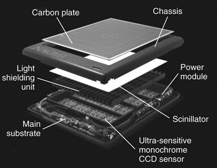
The oldest indirect-conversion digital radiography systems used charge-coupled devices (CCDs) to acquire the digital image. These devices are still being used in a variety of image capture applications. In a CCD system, x-ray photons interact with a scintillation material and the signal is transmitted by lenses or fiber optics to the CCD. During the transmission process, the lenses reduce the size of the projected visible light image and transfer the image to one or more small capacitors that convert the light into an electrical charge. This charge is stored in a sequential pattern and released line by line and sent to an analog-to-digital converter (ADC) (Figure 6-1).
Structure and Function
A photosensitive receptor and electronics embedded into a substrate material in a silicon chip make up a CCD. Incident light from a scintillator strikes the detector and electron/hole pairs are produced in the silicon. The number of electron/hole pairs is related to the amount of light that is absorbed. The electrons are held by electrostatic forces in the array until the charge is read out to form the image. The chip is made up of a polysilicon layer, a silicon dioxide layer, and a silicon substrate (Figure 6-2). The polysilicon layer is coated with a photosensitive material and contains the electronic gates. The silicon dioxide layer is an insulator and the silicon substrate contains the charge storage area.
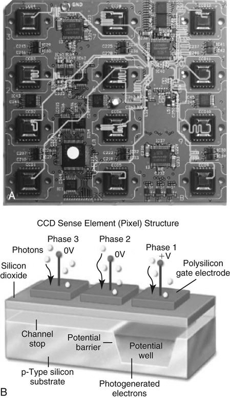
Each pixel or detector element (del) contains three electrodes that hold the electrons in a electrical potential well. The dels are formed by voltage gates that, at readout, are opened and closed like gates to allow the flow of electrons. To collect the charge on the silicon chips, the voltage sign is changed on the electrodes within each del, moving the electrons by rows down the columns until the readout row is reached. This process is commonly known as the “bucket brigade scheme” (Figure 6-3). Once the readout row is reached, the data are sent sequentially to the sense amplifier and are then digitized. The readout process requires that the movement of the electrons is timed, and multiple voltage changes occur; however, the process is very quick. There can be issues with overfill in the dels, which causes excess electrons to spill out of the del into an adjacent del. This is handled by building overflow drains into the array to reduce or prevent this “blooming” effect.
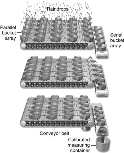
Image-Related Characteristics
Because of the high cost of a CCD chip, it is not practical to manufacture CCD chips any larger than 5 cm × 5 cm. Most chips range from 2 to 4 cm. The image has to be matched to the size of the CCD, which implies that the image must be reduced in size. To do this, CCD technology uses lenses or fiber optics so that the image matches the receptor size. Reducing the image size involves several factors that contribute to the quality of the image and each must be considered. These factors include the scintillator, light collection components, and noise.
The Scintillator.
The type of scintillator and the way it is constructed will determine how much of the incident x-ray photons are absorbed, how much light is produced, and the wavelength or color of the light. Remember from Chapter 5 that there are two main types of phosphors: structured and unstructured (turbid). An unstructured phosphor will produce more light spread when stimulated by x-rays, thereby decreasing the efficiency of the detector. Gadolinium oxysulphide (Gd2O2S) is considered an unstructured phosphor because of its powderlike grains and cesium iodide (CsI) is considered a structured phosphor because of its needlelike crystals.
CCD systems may use the same scintillator as amorphous silicon technology thin-film transistors (TFTs); CsI is a particularly common scintillator. The CsI needles focus light onto a very narrow area, reducing light spread and allowing the use of thicker scintillators without losing too much spatial resolution.
Lenses and Fiber Optics.
Lenses or fiber optics are used to focus light onto the CCD chip. The efficiency of the transportation of light to the chip becomes very important because of the noise created. The more light that is sent to the chip without the creation of noise, the more efficient the system is. The design of the optics is crucial in imaging performance because of the issues that arise with geometric distortion such as light scattering or lens or optics flaws. The ways that physicists and manufacturers determine the efficiency of lenses and fiber optics involve complicated mathematical formulas that are beyond the scope of this text. However, it is important to acknowledge that optics in a CCD are critical contributors to the quality of a digital image and must be considered when evaluating image capture technology.
Detective Quantum Efficiency.
The amount of electrons produced relative to the incident light from the scintillator is the quantum efficiency of the CCD. The quantum efficiency represents the absolute efficiency of the light collection and the signal created in the chip. This is not detective quantum efficiendy (DQE; ratio of output signal to signal-to-noise ratio), but quantum efficiency does have an effect on DQE.
The CCD device is built to be as efficient as possible. The polysilicon layer must be transparent enough so that light passes through it to reach deeper into the substrate storage area, but not so deep that it cannot be captured in the potential well. Also, the spectrum sensitivity of the CCD must match the spectral output of the phosphor. The less sensitive the CCD is to the light spectrum of the scintillator, the less efficient the CCD is.
Noise.
There are several types of noise associated with CCD technology; statistical noise, “dark” current noise, and amplification noise are three common types.
Statistical noise is noise created by the lack of light photons from the scintillator. If there are not enough x-ray photons striking the scintillator, or if too few light photons are produced by the scintillator, then too few electrons will be generated and the output signal will be noisy (quantum mottle). Dark current noise occurs when the CCD chip operates without radiation stimulation. This happens when the temperature rises and electrons are moved into the bulk silicon or depletion area and are stored until readout occurs later, adding unnecessary information to the image. Some manufacturers add a thermoelectric cooling device that can reduce the temperature as much as 40° F lower than room temperature. Because dark noise can be as much as 10,000 electrons/pixel per second, and a 40° drop can reduce dark noise by a factor of 100, temperature consideration is very important.
Amplification noise is common to digital systems. Even though a CCD is one chip, the process of manufacturing that chip is extremely complicated and the response of each chip will vary across the array. Some pixels may not work at all and although software is used to correct the statistical variation because of inoperable pixels, the more bad pixels, the worse the detector efficiency. Because the manufacturing process is so complex, there are no CCDs without amplification noise; however, the number of defects rises as manufacturing costs decrease. The lower the cost of the CCD, the higher the number of defects.
CCD Applications
CCDs are used in several applications in radiology including digital fluoroscopy, stereotactic breast biopsy, digital mammography, and general radiography. In digital fluoroscopy, the CCD is a great replacement for the television (TV) pickup tube in an image intensifier because the CCD size (2 to 5 cm) is closely matched with the output phosphor of an image intensifier (1 inch). The CCD readout is linear and has a greater dynamic range than a TV tube; because oversaturation is almost zero, blooming is greatly reduced, shortening the recovery time from one image to another. CCDs are much more compact than TV tubes and CCDs are not susceptible to electron scanning errors the way that TV tubes are.
For stereotactic breast biopsy applications, a single CCD detector can be used because the typical field size is 50 mm × 50 mm. However, most current systems use a 2.5 cm × 2.5 cm chip that results in some demagnification. Demagnification is the process of reducing the phosphor output image to the size of the active area of the CCD chip. The demagnification uses lenses, optics, and mirrors to accomplish this task. Because of the low dose, noise is not much of a factor. In digital mammography, early applications used CCDs, but these applications are being replaced by flat-panel systems.
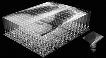
In general radiography, CCDs may be tiled in a 16 × 12 array (Figure 6-4) to a single CCD. CsI is common as the scintillation material. Another way CCDs are used is in a whole-body scanner, where 12 CCD cameras are coupled to gadolinium sulfur dioxide scintillators with tapered fiber optics. The tube and receptor array are housed in a C-arm type of mount and the body is scanned by a moving fan-beam (slot-scanning device) down the length of the table. The scan can be any length up to 180 cm. The table is actually a stretcher and is largely used for trauma applications and forensic pathology.
CCD Advantages and Disadvantages
CCDs are relatively inexpensive compared to TFT-based flat-panel systems and much more simple. They are modular, making them easy to repair, replace, and upgrade. Advantages and disadvantages depend greatly on the application as noted previously. The strongest advantage of CCDs is their modular design, and the greatest disadvantage relates to demagnification issues and reduced DQE because of the demagnification.
Complementary Metal Oxide Semiconductor (CMOS) Systems
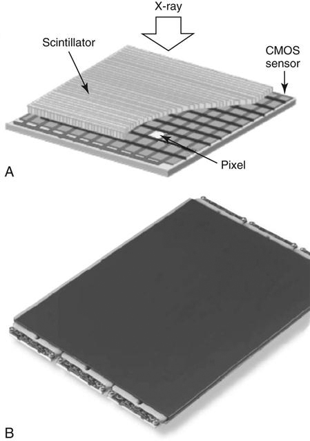
Developed by NASA, complementary metal oxide semiconductor (CMOS) systems use a scintillator that, when struck with x-ray photons, convert the x-rays into light photons and store them in capacitors (Figure 6-5). Each pixel or detector element has its own amplifier, which is switched on and off by circuitry within the pixel, converting the light photons into electrical charges.
Voltage from the amplifier is converted by an ADC. This system is highly efficient and takes up less fill space than CCDs. CMOS is a semiconductor. A semiconductor is a solid chemical element or compound that conducts electricity under some conditions but not others, making it a good medium for the control of electrical current. Its ability to conduct current varies depending on the amount of current or voltage it receives or on the intensity of radiation by x-rays. Impurities (also known as dopants) are added to semiconductors because the materials semiconductors are made from do not conduct electricity very well by themselves. Thus they are “doped” with impurities that make them highly conductive.
Typical semiconductor materials are antimony, arsenic, boron, carbon, germanium, selenium, silicon, sulfur, and tellurium. Silicon is the most popular and is the base material of most integrated circuits. Common impurities added to the silicon are gallium arsenide, indium antimonide, and oxides of most metals. When doped, the semiconductor becomes a full-scale conductor or becomes an N-type transistor (extra electrons with a negative charge) or positive charge carriers (P-type transistors). In most semiconductors of the CMOS kind, both types of transistor are used so that they form a gate that can be controlled electrically. Although CMOS transistors use little to no power when they are not in use, if the direction of the current changes rapidly, the transistors become hot and this slows down the microprocessors.
Like CCD technology, CMOS image sensors convert light into electrons. The electrons are stored in capacitors located within the pixel. During readout, the charge is sent across the chip and read at one corner of the array. This is typically done using several transistors at each pixel that amplify the charge and send it through wires to the array corner. An ADC turns each pixel’s value into a digital value.
Comparison between CCD and CMOS Technology
There are some noticeable differences between CCD and CMOS sensors.
• CMOS sensors are more susceptible to noise.
• CMOSs are very inexpensive to manufacture compared to CCD sensors.
Despite their differences CCD and CMOS technologies both provide excellent image capture capabilities; also for both, their usefulness depends on the type of application. Each has strengths unique to those applications and neither is superior to the other.
Current CMOS designers are working diligently to increase image quality and CCD designers are seeking to decrease power requirements and pixel sizes. Both of these technologies continue to be improved year after year because of their wide use in many industries. Medical imaging will continue to see growth and new applications from both CCD and CMOS detectors.
Summary